Hdl Gate Level Description
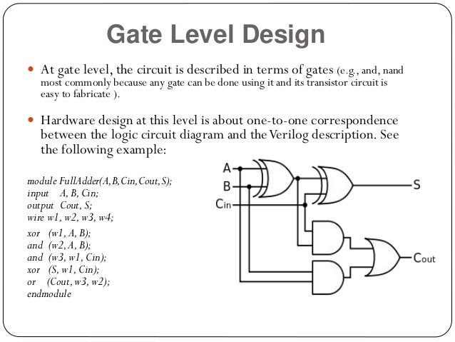
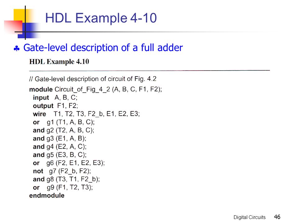
Hdl Example 4 10 Gate Level Description Of Circuit Of Fig 4 2 Module Analysis A B C F1 F2 Input Ppt Download

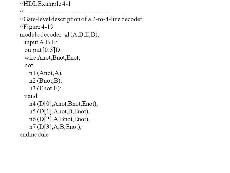
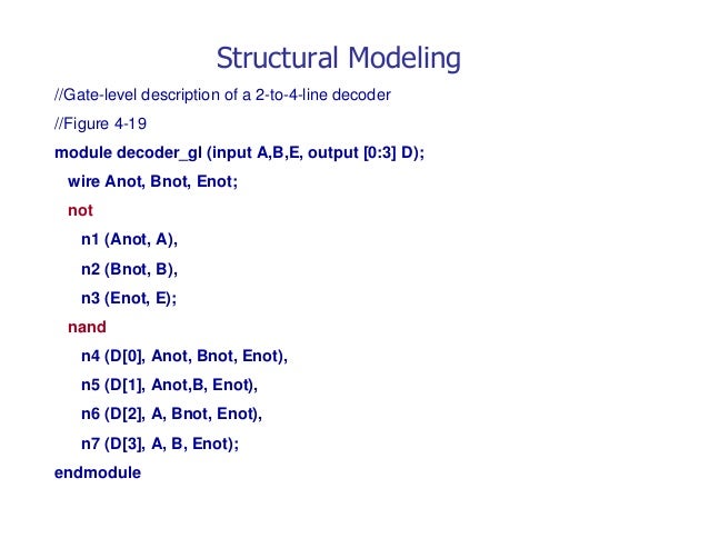
Structural Gate Level Description Of Decoder
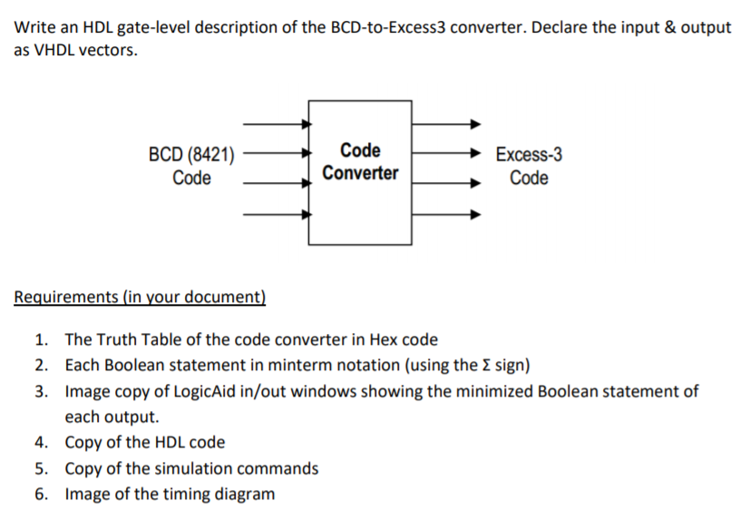
Write An Hdl Gate Level Description Of The Bcd To Chegg Com
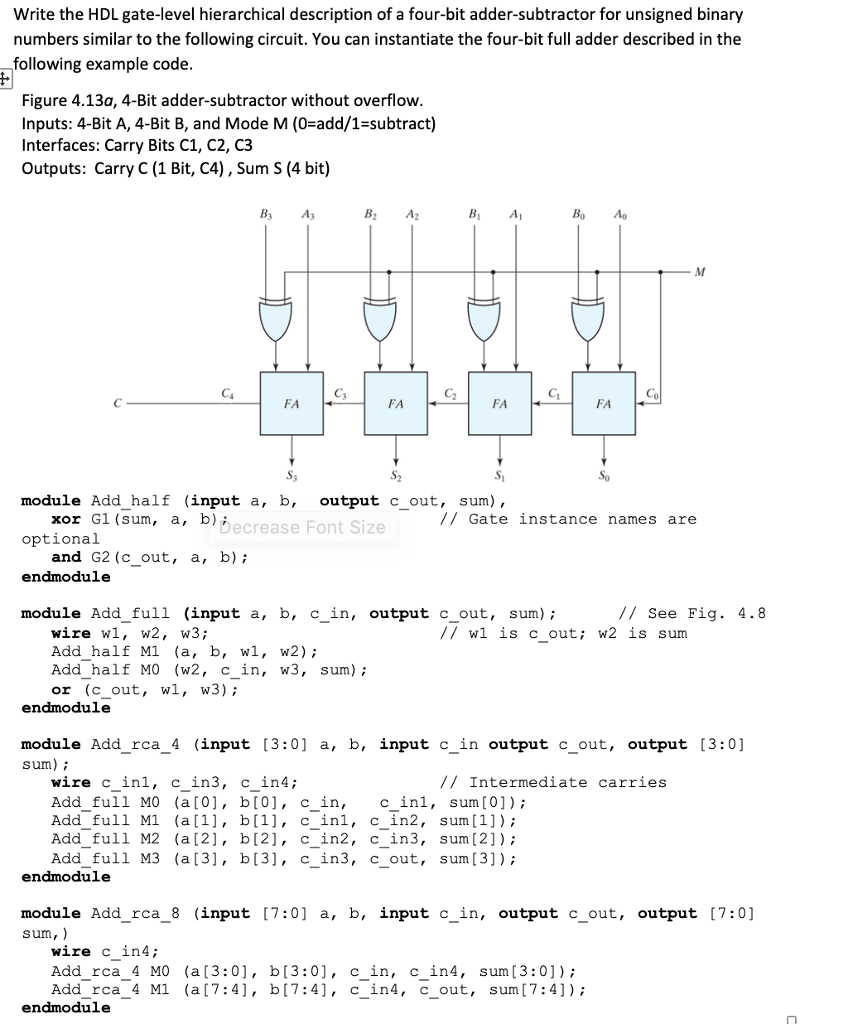
Solved Write The Hdl Gate Level Hierarchical Description Chegg Com
Solved Write The Hdl Gate Level Description Of The Priori Chegg Com

Hdl Example 3 3 Stimulus For Simple Circuit Module Stimcrct Reg A B C Wire X Y Circuit With Delay Swd A B C X Y Ppt Video Online Download
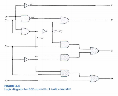
C write an hdl behavioral description of a bcd to excess 3 converter.
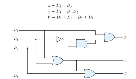
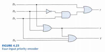
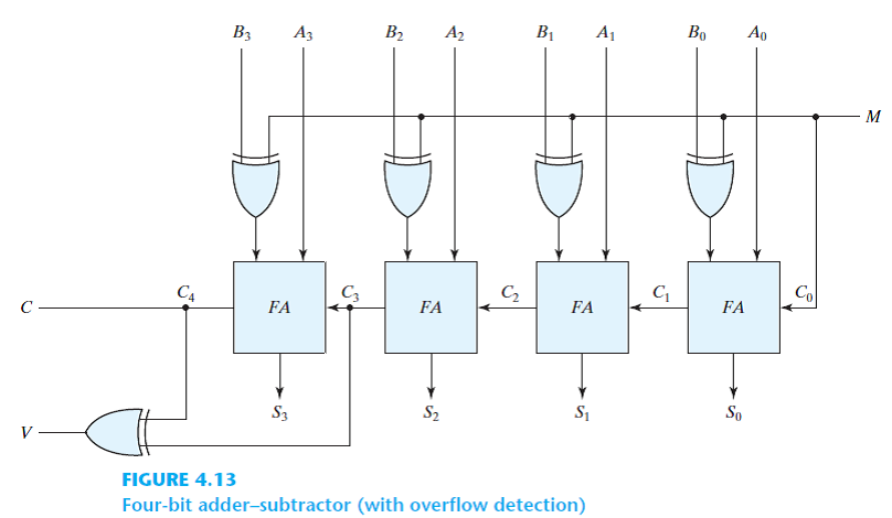
Hdl gate level description. Write the hdl gate level hierarchical description of a four bit adder subtractor for unsigned binary numbers. Please subscribe to my channel. D d d v do figure 4 23 four input priority encoder 8 find the syntax errors in the following verilog code. Circuit shown in fig.
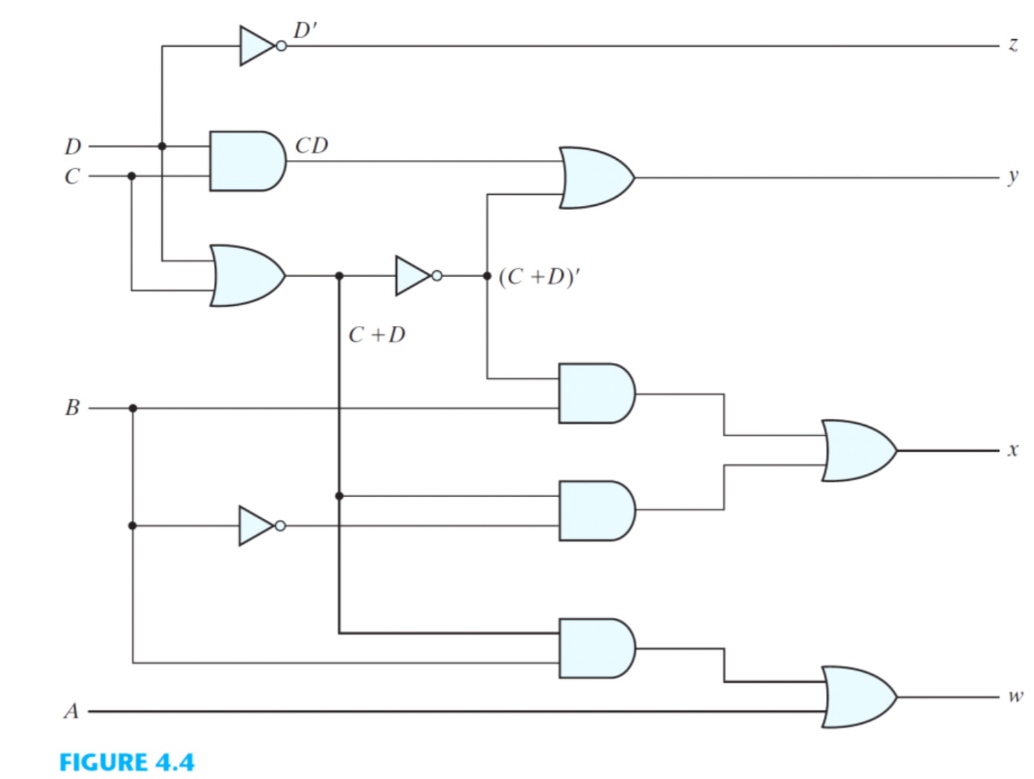
Write the hdl gate level description of the priority encoder circuit shown in fig. Hdl example 3 1 hdl description for circuit shown in fig. 4 4 see problem 4 22. 57 gate displays example.
On the logic level the design is represented as a netlist with logic gates and or not and storage elements. Note that names for primitive or primary logic gates are optional. 59 hdl example 3 3 test bench for simulating the circuit with. You can instantiate the four bit full adder described in hdl example 4 2.
The importance is given to making concepts easy. 4 4 see problem 4 22. B write a dataflow description of the bcd to excess 3 converter using the boolean expressions listed in fig. D write a test bench to simulate and test the bcd to excess 3 converter circuit in order.
In structural modeling style we defines that how our components registers modules are connected to each other using nets wires. Vlsi design specification using verilog hdl study material lecturing notes assignment reference wiki description explanation brief detail. Small description about gate level modeling style in verilog hdl. The circuit is similar to fig.
B write a dataflow description of the bcd to excess 3 converter using the boolean expressions listed in fig. Structural modeling style structural modeling style shows the graphical representation of modules instances components with their interconnection. For the description on rt level only 10 to 20 percent of all vhdl language constructs are needed and a strict methodology has to be followed. A write an hdl gate level description of the bcd to excess 3 converter circuit shown in fig.
Write an hdl gate level description of the bcd to excess 3 converter circuit shown in fig. This description on rt level is called synthesizable description. 58 hdl example 3 2 gate level description with propagation delays for. Wish you success.
8 write the hdl gate level description of the priority encoder circuit given below figure 4 23.
Get Answer Write The Hdl Gate Level Description Of The Priority Encoder Transtutors
Solved A Write An Hdl Gate Level Description Of The Bcd Chegg Com

Hardware Description Language Hdl
Verilog
Combinational Logic Digital Circuits Introduction Logic Circuits For Digital Systems May Be Combinational Or Sequential A Combinational Circuit Ppt Download

Verilog Ppt Download

Http Www Ee Ic Ac Uk Pcheung Teaching Ee2 Digital Lecture 203 20 20verilog 20hdl Part 201 20 X2 Pdf
Solved Write The Hdl Gate Level Hierarchical Description Of A Chegg Com
Verilog Tutorial
Get Answer A Write An Hdl Gate Level Description Of The Bcd To Excess 3 Transtutors

Terms Relevant To Verilog Hdl Module Test Bench Page 1 Of 12 Logic Gate Hardware Description Language

Veriloghdl Basic Half Adder Using Gate Level Modeling Youtube